
|
|
4QD-TEC
|
|
It is not at all difficult to make an op-amp using transistors. This page shows you how and discusses how they work. I am not giving all circuit values here, just enough to describe operation. Actual circuit values will depend on exactly what you want to do with the circuit. Anyway, it's not necessary to have circuit values when you're trying to gain an understanding of how the circuit works.
But you will find links to other circuits on this site which use these op-amp as a building block.
The first circuit illustrates about the simplest possible implementation. It's shown here as it might be used from a single supply voltage.
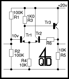
Consider the circuit running from, for ease of understanding, a 20v supply, but the actual value doesn't affect the discussion. R1 and R2 will be equal values, maybe 100K, so the voltage at the base of Tr1 will be 10v: in effect we have made a 'centre reference' voltage with the top and bottom supplies at +10v and -10v.
Now we know (don't we?) that the voltage between the base and emitter of a transistor is around 0.6v. So the emitter of Tr1, for it to work, must be around 9.4v. There must be, then, just under 1mA flowing through R4 to establish this current, The current through R4 can only reach it by flowing from the emitter of Tr1 or Tr2 in some ratio.
The current flowing in Tr1's emitter must also be flowing in its collector, i.e. coming from the 20v supply via R3. In flowing through R3 it develops a voltage across R3, which will be about 0.6v if Tr3 is to conduct.
If Tr3 conducts more, it increases the current flowing in R5, increasing the voltage dropped across R5. But if the voltage across R5 rises, it will raise the voltage fed to the base of Tr2 which will cause Tr2 to conduct more.
So the circuit balances itself, with the current in R4 split between Tr1 and Tr2, with just enough current flowing in Tr1 to cause Tr3 to 'balance' the output voltage so that it is equal to that on the input.
The simple circuit is fine but if you followed the description, you will realize that, if the input voltage changes, the emitter voltage also will change (as it has to follow the input) so also the current through R4 will change. R4 is reducing the effect of the input voltage changes. Also the output voltage change will cause a current change in Tr3, as the current in R5 will depend on the output voltage. In effect some of the wanted output current is being wasted in R5.
To reduce the effect of the signal currents flowing on R4 and R5, we need to make these resistors as high as possible - but their values are fixed by circuit constraints! However, there is a way! Look at the next circuit.
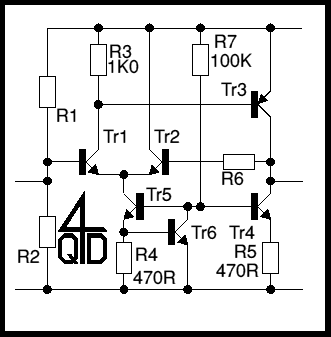
In this, R4 has been replaced by a constant current source (or, to be pedantic, a current 'sink' as current if flowing into in), Tr5 and R5 by another current source, Tr4. If you don't understand current sources seeCurrent sources and mirrors. The current in Tr5 is constant, unaffected by the voltage on its collector so the wanted signal voltage only changes the balance of current in Tr1 and Tr2, not the combined current. This dramatically increases the overall gain of the circuit. The same consideration also applies to Tr3's current, now unaffected by R5.
If you look at the equivalent circuit of almost any op-amp, you should recognise this basic circuit format. Of course, ours is quite simple: IC's use al manner of extra ideas to enhance performance. Also many common IC's turn this basic circuit upside-down, using PNP input transistors, so that he input voltage can be at the zero volts rail and the circuit will still work.
Believe it or not, the circuit which follows is in many respects the same as the two described already though it looks entirely different and possibly somewhat simpler. It is a circuit which is original to me and I have never seen its like used elsewhere!
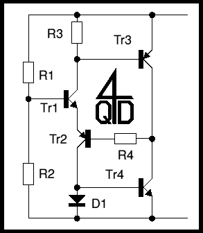
This op-amp has some surprising properties! Surprisingly enough, Tr1 and Tr2 are actually a long-tailed pair (LTP). This may make you think a little, but study the circuit. The LTPs you have seen all use two identical transistors (NPN or PNP) with their emitters coupled. These two are complimentary (one PNP and one NPN) with their emitters coupled. The current through both is the same at all times - and it doesn't use a constant-current source to do this!
As with the above circuits, R1 and R2 establish a base voltage for Tr1 and Tr1's collector current flows in R3 establishing a base voltage for Tr3. Tr3's collector current is determined (the long way round) by Tr4 which a current source, biased by the current in Tr1 and Tr2, flowing through D1. Since Tr3 is operated at constant current, its base-emitter voltage is well defined, so the current through R3 is well defined, hence the LTP current. This is turn supplies a constant bias for the current source reference diode.
There are (always) trade-offs. The base-emitter voltages of Tr1 and Tr2 add rather than cancel, so it's not good for d.c. applications. But it's extremely simple and can have a surprisingly good performance.
This basic block is actually quite useful and is used in:
| 4QD Sites: |