|
|
4QD-TEC
|
|
Generating a PWM waveform is extremely simple! This page demonstrates a circuits for doing this and discusses some of the considerations. All of the circuits are d.c. input to p.w.m. out.
The first example uses the standard op-amp oscillator circuit to generate a triangular waveform which is level-shifted and fed to a comparator (e.g. LM339) to give the PWM waveform. Most people will want to use two comparators rather than one op-amp and one comparator so that is what we show here.
The triangle wave oscillator is formed around Cp1. Consider the initial state with C1 uncharged. The comparator's - input will be low, so the comparator's output will be high (off) and C1 will charge (from the comparator's output) via R2 and R1. The comparator's +ve input will be biased to about 2/3 of the supply voltage (Vcc) since R5 is, in effect, in parallel with R3.
So, when C1 charges above 2/3 of the Vcc, the comparator will turn on, its output going low. R2 will now start to discharge C1. But R5 is now effectively in parallel with R4, so the positive input is only biased at about 1/3 of Vcc
It should be clear that the comparator will again change state when the voltage on its + input falls below 1/3 Vcc and the waveform on C1 will be a triangle waveform rising between 1/3 and 2/3 Vcc.
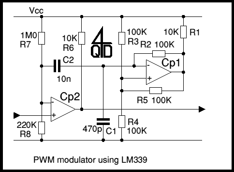
C2, R7 and R8 form a level shifter. Ideally the negative tip of the waveform should fall to very nearly zero volts - just enough so that a zero input will always cause Cp2 to turn fully off, so the circuit may take a bit of fiddling to get the exact levels, or you have to accept a small dead band at zero speed, which is not usually a problem.
The triangle wave is slightly non-linear because of resistive charging and discharging between 1/3Vcc and 2/3Vcc. Non linearity can be reduced by making the thresholds closer to 1/2Vc: for instance increasing R5 to 200K would reduce the triangle waveform amplitude. You would also have to alter the level shifting appropriately!
This is similar to the first circuit but the two resistors R2 and R5 of the first circuit have been replaced by diodes. This is a modification that was triggered by a customer's suggestion, but the details are all our own!
At power-up, C1 is discharged and starts to discharge via R6. + input to Cp1 is held at approximately 1/3 Vcc by R1 and R2. C1 charges up to this level and the comparator switches on, pulling its output low.
C1 now discharges through D1 and D2 holds the junction of R1 and R2 at one Vd above zero volts. When C1 is sufficiently discharged the current through D1 is limited by R6 whilst the current through D2 is limited by R2, so will be 10 times as high as that through D1. Because of this current ratio, it can be guaranteed that there will be less voltage dropped across D1 than across D2, so the negative input will always fall below the positive input and the oscillator will always reset.
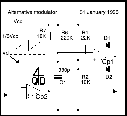
The circuit has several advantages
To offset these advantages, the oscillator gives a sawtooth rather than a triangular waveform but there are very few occasions when this has any practical significance.
The 555 can be used, on its own, as a modulator. However it is not possible to vary the modulation from zero to 100%, which limits its usefulness. However you can use a 555 as a sawtooth oscillator and the next circuit illustrates this.
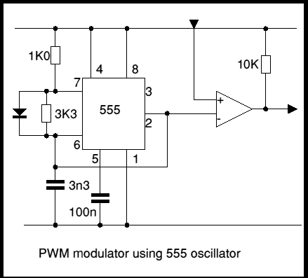
You will see that the second circuit (above) has a lower component count!
| 4QD Sites: |