
|
|
4QD-TEC
|
|
This is a page of analogue interfaces for joysticks. Although these interfaces have been developed for use with 4QD's controllers they will have plenty of other uses. Also because of the development history, we have printed circuit boards available (either fully populated and tested) or bare boards) for these interfaces.
All of 4QD's Motor Controllers require a speed input (typically 0-4 volts) and a separate direction input, so that is what these interfaces provide. Circuits are provided but as some of these are quite large, as links rather than as embedded GIFs. The index allows you to jump direct to the appropriate section.
Single axis interface
The first interface is a single axes for the type of control often referred to as 'Wig-Wag': centre is off, move the input pot forward to move forward and backwards to reverse.
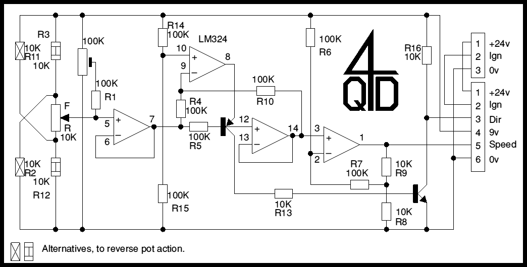
Since this circuit is also used in all the other versions of the interface I will give a detailed description of its operation. This one is intended for use with 4QD's NCC or Pro-120 series controllers which use a 9v internal supply, so the circuit is powered from this. However the supply voltage is not critical.
On the left is the 10K pot with a 10K in series with each leg, so that swinging the pot from maximum to minimum will swing the wiper from 3v to 6v. The centre position will be 4.5v, with a ± 1.5v swing. R3 and R12 are normally fitted but, on 4QD's circuit board, R10 and R2 may be fitted instead to reverse the action of the potentiometer.
R1 and the preset are optional and are for centring the input. However that is always best done by mechanical adjustment so the mechanical centre and true electrical centre coincide. These components also mean that, if a wiper wire to the input pot breaks, the circuit does not go to full speed but remains at zero (centre).
The IC used is a quad op-amp such as LM324. The first stage simply buffers the pot wiper. So we get 4.5v ±1.5v on pin 7. This is fed to the second and third sections of the chip which form a precision rectifier circuit. To understand this, consider only the base-emitter junction of the PNP transistor, which is used as an ordinary diode.
Pin 10 of the IC is biased at 4.5 volts (the zero point) via R14 and R15. If pin 7 rises above this, pin 8 will fall below 4.5v and the transistor diode will be reverse biased, so you can ignore pin 8/9/10 section of the IC for positive swings.
Pin 7 feeds via R5 to pin 12 of the IC, which is a unity gain follower - so positive input swings (above centre point) are followed through to pin 14.
Negative swings cause a positive excursion of pin 8 so the transistor diode immediately goes into conduction and pin 8 is coupled though the diode to pin 12 which is unity-gain followed through to pin 14. So pin 14 is (one diode below) pin 8. The section 8/9/10 now becomes a unity gain inverting amplifier with gain determined by R4 and the feedback resistor R10. So for negative swings, the excursion is mirrored into a positive excursion at pin 14.
Pin 14 therefore goes positive of centre point for negative excursions and positive also for positive excursions of the input, both with overall unity gain, so it gives a rectifying action. Aka 'Absolute value amplifier, or 'Precision rectifier'.
Now here's the crafty bit (which as far as I know is original to the author): When the transistor's base emitter diode is forward biased, current can also from out of pin 8 through the now-turned-on transistor and through R13 into the base of the direction output transistor. So this second transistor switches off for positive excursions and on for negative excursions. This gives a direction indication output with very few extra components!
The last section of the chip is a level shifter: pin 2 is a potential divider R6 to positive and R7 to the junction of the 2 10K resistors R8 and R9. Pin 3 is at half rail (for zero excursion). So the junction of R8 and R9 must be at 0v for zero excursion.
Actually, because the parallel value of R8 and R9 is 5K, the effective bottom-end resistor is 105K, so the circuit will want to go slightly below zero. It cannot - but the effect will be to introduce a small 'dead-band' of 5% as the swing has to move 5% to bring this point exactly to zero. It also slightly alters the gain calculation.
At this 5% point, the IC starts to operate and raises pin 1 as required to keep pin 2 at the same potential as pin 3. For a 1.5v swing, the junction R8/R9 will have to rise by 3v: if pin 3 rises by 1.5v, pin 2 must follow it so the current through the R6 must reduce. To balance it, the current through R6 must all flow through R7, so a 1.5v rise at pin 2 must cause a 3v rise across R8.
For R8's voltage ro rise to 3v, Pin 1 must rise by 6v - so we have a gain of 4 times here, set by R8 and R9.
The two connectors are a 6 way, designed to mate with 4QD's NCC series controllers, and a 3 way which is used to power up the NCC's ignition circuitry.
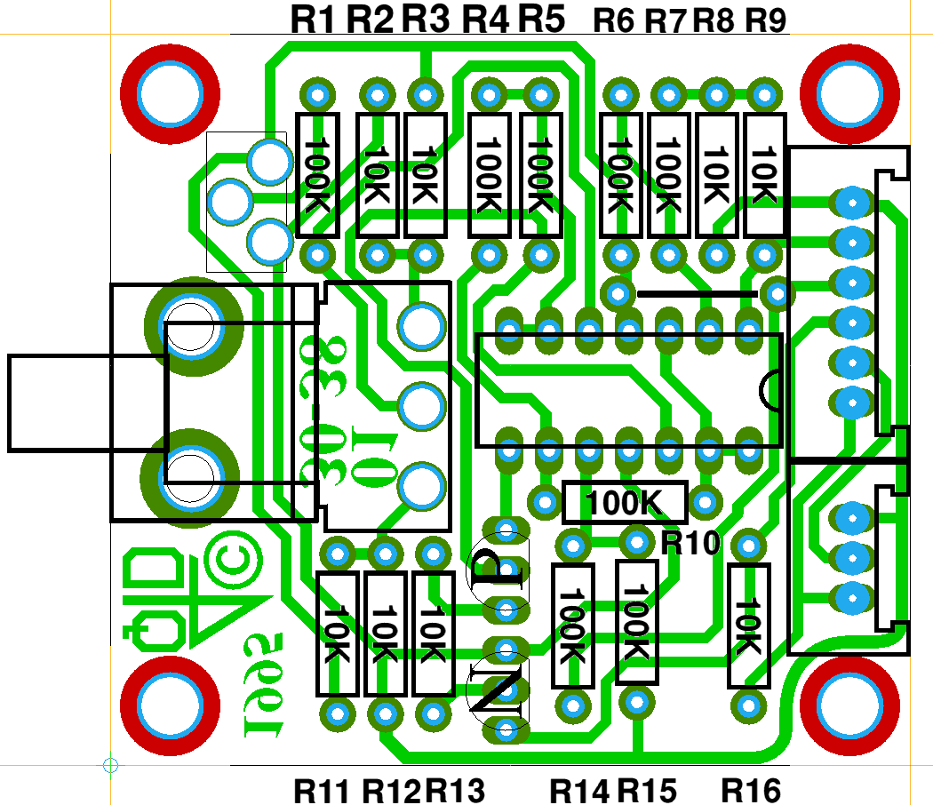
A 65K GIF of the layout of 4QD's assembly of this circuit which 4QD can supply as:
See also Joystick Interfaces
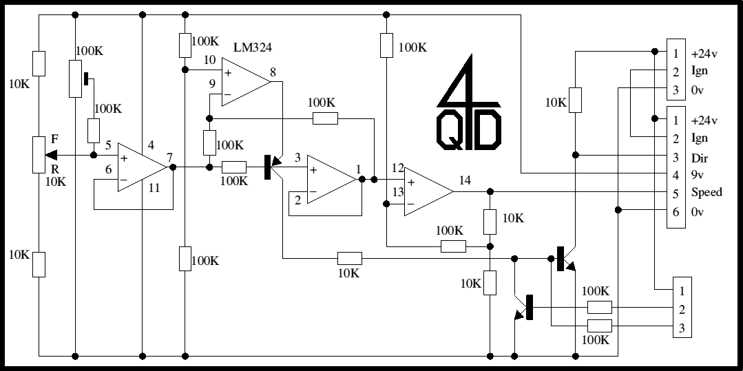
Single axis interface: daughter version
this is another version of the single-axis interface which, instead of mounting on the pot, mounts on the NCC series controllers. This makes it possibly of less use to most browsers, but what may interest is the way of adding end stops. An additional three pin connector is present. If a voltage is applied to pin 3 (via a travel limit switch), the reverse transistor is turned on (when the direction is. If a voltage is applied to pin 2, the reverse transistor is turned off. The NCC series controllers are dual-ramp, so if the direction is changed whilst the motor is powered, the controller will ramp down, stop and then start up in the opposite direction. So pin 2 must be the end stop which is activated in the forward direction, pin 3 is the reverse end stop.
Circuit of daughter version 22K GIF.
See also Joystick Interfaces for a drawing of the interface.
Dual axis interface: sum and difference version
Since this is a circuits archive, many readers will be interested in the circuits, so the following sections (which refer to the issue 1 DXI) are retained although the circuit has been changed somewhat for the more recent DCI-111 - the circuit of this follows later on.
This is a two axis version for use with a standard resistive (or contactless, inductive) joystick to drive two controllers, each operating a separate motor. Moving the stick forward and backwards affects each motor equally for movement in a straight line. Moving from side to side speeds one motor and slows the other allowing vehicle steering by differential control. The circuits of these interfaces get quite large so if you want to download them, click on the links.
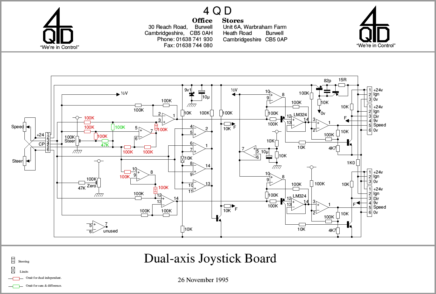
This description refers to Circuit of Dual axis sum and difference board , 46K GIF. You should immediately notice that the right hand end consists of the single axis circuit, duplicated. That circuit's operation is described above, so will not be repeated.
Power supply is a current source (top right corner) feeding a 9v1 zener: the sources about 50mA: far more than this circuit requires, so that there is enough spare current to feed an inductive joystick. If you don't use one of these you should be able to get away with a 33R instead of the 15R shown in the current source. The power supply section also include one spare quarter of one of the LM324 ICs which used to derive a centre reference voltage (pins 5, 6, 7 of IC4), shown as 1/2V.
IC2 is an 'out of limits' window detector. It is an LM339 measuring the joystick inputs. Normal swing on the stick is ±1v. The thresholds on this detect swings in excess of ±1.5v - which can only occur if the joystick has gone faulty or a wire has broken or shorted. In such an event the transistor is turned on and point F are shorted to 0v: this disables both the NCC series controllers.
Which leaves only IC1 to account for. Sections 1, 2, 3 and 12, 13, 14 are both unity gain non-inverting followers which both will follow the common 'speed' input. The other two sections are set, one with a gain of +1 and the other with a gain of -1, to follow the steering input. These feed into pins 3 and 12 of the speed followers to give a differential effect.
With the values shown, gain on all channels is unity. This would be fine for, say a robot, with rapid 'on the spot' manoeuvring but for an invalid wheelchair the steering would be too vicious. For this use the gain of the differential channels would have to be reduced to diminish the effect. This can easily be done by increasing the value of the two 100K resistors marked, from pins 7 and 8 of the differential op-amps.
Unfortunately (as in most analogue circuits) changing one value has side effects: increasing these resistors to decrease the steering will increase the common (speed) gains, so it may be necessary to alter the gain in the output stages to compensate!
The circuit is shown with resistive pots at the input. These are operating from the 9v rail so, at rest, the centre voltage will be 4.5v. The interface requires ±1v for full swing, which will correspond to 1/9 of the pot travel, i.e. ±30° for a standard pot. This angle can be increased by fitting end resistors.
Dual axis circuit showing changes for double independent board , 59K GIF.
See also Joystick Interfaces for a drawing of the interface.
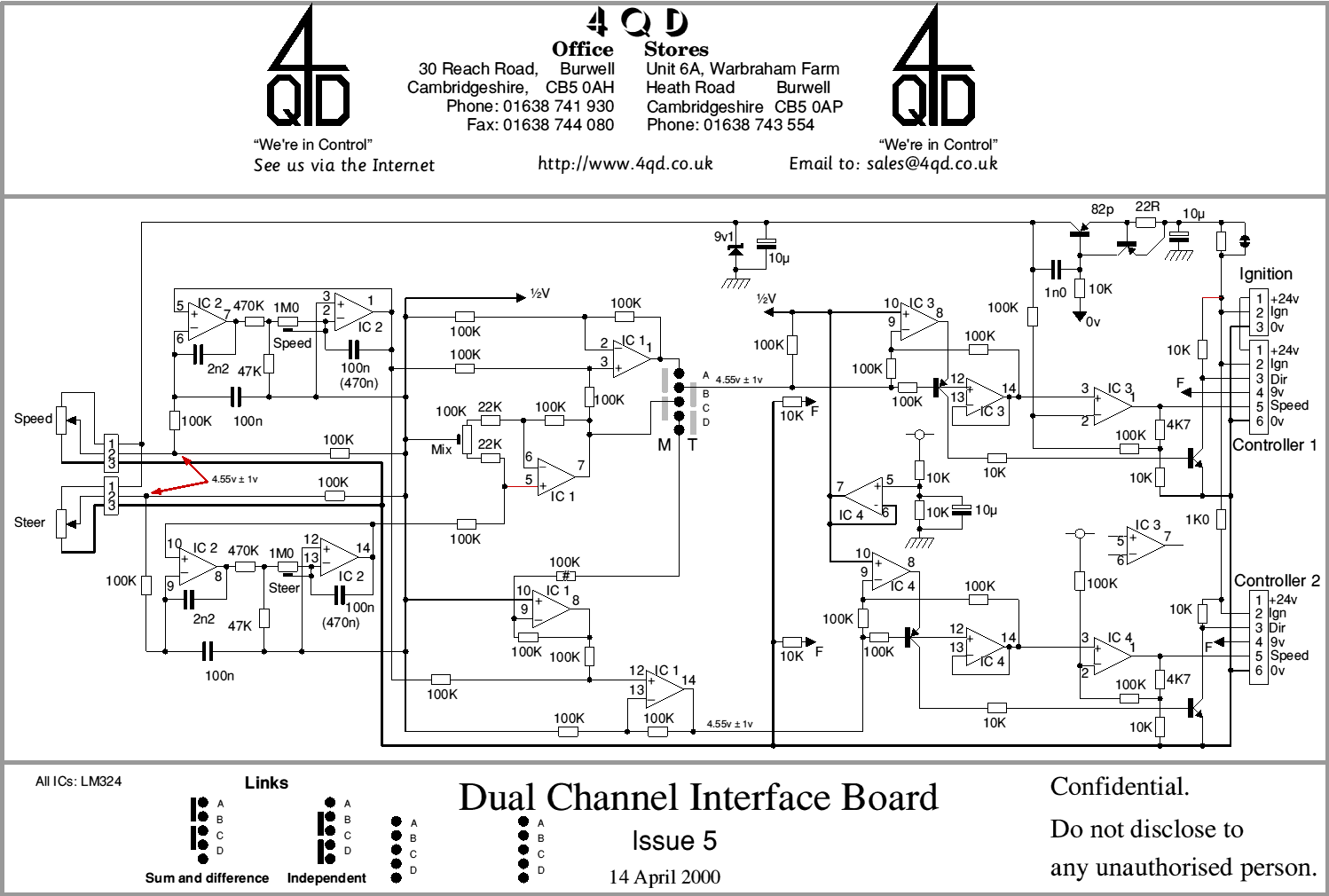
Dual Channel Interface - DCI-111
This is effectively issue 2 of the earlier board. download circuit diagram of DCI-111 (58kB PNG). So the description will refer back to the earlier version.
Right at the inputs of the DCI-111 there are two ramps, one for each axis. These give symmetrical ramping (+ve and -ve) as this seems to suit most machines using the DCI-111. Putting the ramps at the input reduces setting up, as one setting affects both channels equally.
The ramps are integrators - the 100n (or 470n) is the integrating capacitor - with overall unity gain at d.c., so they give a controlled slew rate.
IC1 (12,13,14) and IC1 (1,2,3) both follow the 'speed' channel. IC1 (5,6,7) follows the Steer channel with its output being inverted by IC1 (8,9,10). However this mirroring is via the pinstrip header so that IC1 (8,9,10) only gives a mirror if the pins are linked as shown by the right grey links. Otherwise Pin 8 is at half supply rail.
With the pins in this position, IC1 (1,2,3)'s output is fed to one channel and the steer signal and its mirror are mixed to give differential steering.
With the pins in the right hand grey position, the top channel feeds independently of the 'steer' input and there is no mixing. However IC1 (5,6,7) is still affected by the mix control, which will simply alter the gain. So he mix control should be left centred to keep the two channels balanced.
Pages relevant to this subject
| 4QD Sites: |